| Author | Message | ||
South Hills ARC Username: Admin Registered: 03-2006 |
By Jim Mounts - KA3EBX I sure wish I had been paid for every printed circuit board I ever made over the years. When I first started working in 1983 for ITS Corporation, a television transmitter manufacturer, I spent about 50% of my time designing, hand etching and building printed circuit boards. Many of these boards were actually shipped in transmitter products to television stations all over the country. At that time, we didn't have high-tech printed circuit board design software. In fact, we didn't even have a computer! As a new company, we were always striving for new business and quoting incredibly fast delivery to our customers which often forced us to make many of our printed circuit boards by hand to cover our initial orders. For long term solutions, we often hired an outside printed circuit board Draftsman to lay out our boards and we used Triangle Circuits in Pittsburgh to manufacture our boards. However, I didn't learn the technique of printed circuit board layout and etching at ITS Corporation, or with my previous employer, Control Systems Research / Contraves. I learned it through Amateur Radio! In my late teens, I had teamed up with a fellow friend and ham, Jeff Fall, KB3W and we put a 2-meter repeater on the air. Originally, we used a TRS-80 as a repeater controller. We eventually decided to replace the computer with a home-brew controller with plug-in cards and motherboard. Over 20 years later, even though we have swapped out the original tube repeater with a solid state unit, the controller is still alive and well. To make a printed circuit board, you will need the following materials: 1. Copper clad board material 2. Etching solution (Ferric Chloride) 3. Plastic tray for the etching solution 4. Black Sharpie marker 5. Adhesive masking tape 6. Dry transfer decals 7. Brillo Pad 8. Tinning solution (Optional) Copper Clad Board Material: There are many different types of copper clad PCB material. You can purchase single or double-sided board material with various thickness of copper and types of board substrate. If you are making a board that will use logic or analog devices such as OP amps, single-sided board material with fiberglass substrate (type G-10 .062" thick) will suffice. If the board is designed to carry RF or will be used in or around RF energy, double-sided board material is highly recommended. For higher RF frequencies, the board substrate may have to be Teflon rather than fiberglass. Etching Solution: There are several types of solution available, but you will probably find Ferric Chloride more readily available. Most Radio Shacks carry this item. The part number is 276-1535 and sells for $3.99 for a 16 ounce bottle. This chemical is highly corrosive and will stain clothing, so make sure you are wearing something to protect your clothes. If you spill any on a counter, be sure to clean it up right away and make sure you wash your hands thoroughly, as some people's skin may be sensitive to Ferric Chloride. 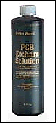 Plastic Etching Tray: The keyword here is "plastic". Don't ever use a metal or foil tray! Ferric Chloride will eat right through it, causing it to heat up and you'll soon have a mess all over the table and floor! Sharpie Marker: A black wide tip Sharpie marker is great to cover large areas of copper that you want to protect from being etched away by the Ferric Chloride. Make sure that you coat the copper well enough so that you can't see the bare copper color underneath. Wait a few minutes for it to dry and go over the area once again with the marker. Adhesive Masking Tape: Once I am done with the Sharpie Marker, I cover these same areas with masking tape. This is like an insurance policy to make sure the solution stays out of the protected areas. You can use scissors or an Exacto knife to cut the tape into smaller strips. Dry Transfer Decals: They say a good product will last the test of time. This is one of them. Radio Shack sells a pack of dry transfer decals that are invaluable for making PC boards. The part number is 276-1490 and sells for $1.99. 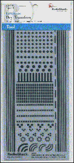 With these decals, you will be able to createstraight and curved circuit traces. They also include decals for laying out IC's, resistors, capacitors and transistors. I have always had great success with these decals. They provide very crisp traces after the etching process. All you have to do is lay the sheet over the board and use a pencil to rub the decal onto the board. Brillo Pad: Before you begin your layout, take a Brillo pad and run it under the faucet to soak it thoroughly. With the water still running, clean the copper clad board with the Brillo pad to remove the clear coating from the copper. If the board is double-sided, be sure to clean both sides of the board. The board should be very shiny and will show minor scratches from the Brillo pad. I also use a Brillo pad to remove all of the dry transfer decals from the board after the etching process. Tinning Solution: Tinning solution is a chemical that is used to coat the copper traces with a protective film. The board is placed in this solution after it has been etched and thoroughly cleaned with a Brillo Pad. The solution changes the copper surface from its original copper color to silver. This prevents the copper from oxidizing and makes the board easier to solder to. Kepro Circuit Systems used to sell this solution, but they just recently went out of business in June of this year. I am sure it is available from other sources. If you can't find the tinning solution, with a low wattage soldering iron, you can coat the traces with solder and wick up the excess with solder wick. If you decide to try this, don't let the soldering iron heat up the trace too long, as it will eventually lift the trace right off of the board and then we'll have to write a new article on PCB repair! Are You Ready to Etch? Although this articles doesn't cover how to design or lay out a printed circuit board, there are layout techniques that can greatly improve the results you will get when etching your board. Personally I like to put all of the traces on the bottom side of the board and leave the topside of the board as solid copper foil. There are two reasons for this. The first reason is that it provides excellent RF shielding to the traces on the bottom side of the board. The second reason is that it speeds up the etching process. Anytime that you have large areas to etch, the board will take longer to etch and you risk the chance of having smaller delicate areas of the board damaged by etching solution creeping under the decals and tape. You want to keep the etching time to a minimum. If there are large unused areas on the board, cover them by using a Sharpie pen and adhesive tape. Once you are ready to etch, pour the solution into the etching tray. Place the board in the solution with the side of the board that has the majority of the traces facing up. Grasp the side of the tray and gently lift up and down so that the solution flows back and forth over the board. There are devices available such as spray etchers, motorized agitators and heat lamps to help aid and speed up the etching process, but if you have the time, simply rocking the tray back and forth will do just fine and save you a lot of money. After about 10 to 20 minutes, you will begin to see the exposed copper areas dissolve and then begin to see the board substrate underneath. Continue to rock the tray back and forth until all of the exposed copper is etched away. Remove the board from the tray and rinse it off under the sink. Using a Brillo pad, remove all of the decals and tape from the board. Clean the entire board with the Brillo pad until it is bright and shiny without any blemishes. If you used the Radio Shack decals, you'll notice that there are etched holes on the solder pads. This is to help guide your drill bit when drilling the holes used to mount your components. Once all of the holes have been drilled, clean the board once again with the Brillo pad. It's now at this point to decide whether or not you want to tin the board. Tinning provides a more professional look and will protect the copper from turning dark due to oxidation. You'll also find it much easier for the solder to adhere to the board when soldering components. If you have any further questions about PCB etching, please feel free to email me at KS3R-AT-sharc-DOT.net |